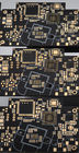
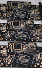
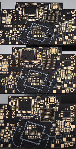
GPS Remote Control Device 1oz 16 Layer Pcb Board With Blind Burried Vias
Production description :
this board is 16layer PCB it is used on GPS remote control device. PCB prototype,samll volum, middle and large volume are accepted. no MOQ request for new boards. All PCB are passed UL, TS16949, ROHS ,ISO9001 etc. Certification.
Key Specifications/Special Features:
| Count : |
16 Layers |
| Base Material : |
FR4 halogen free |
| Copper Thickness : |
1.5 oz in all layer |
| Board Thickness : |
1.0 mm |
| Min. Hole Size : |
4 mil, 0.1mm |
| Min. Line Width : |
4 / 4 mil |
| Min. Line Spacing : |
5 / 5 mil |
| Surface Finishing : |
HAL lead free |
| Certificate: |
UL, CQC, TS16949, ISO14000, ROHS |
| Company type: |
Manufacturer/ Factory |
PCB Flow Chart.pdf
Advantages :
• Strict product liability, taking IPC-A-160 standard
• Engineering pretreatment before production
• Production process control (5Ms)
• 100% E-test, 100% visual inspection, including IQC, IPQC, FQC, OQC
• 100% AOI inspection, including X-ray, 3D microscope and ICT
• High-voltage test, impedance control test
• Micro section, soldering capacity, thermal stress test, shocking test
• In-house PCB production
• No minimum order quantity and free sample
• Focus on low to medium volume production
• Quick and on-time delivery
Technical Capability:
| Item |
Technical Parameters |
| Layers |
1-28 Layers |
| Inner Layer Min Trace/Space |
4/4 mil |
| Out Layer Min Trace,Space |
4/4 mil |
| Inner Layer Max Copper |
4 OZ |
| Out Layer Max Copper |
4 OZ |
| Inner Layer Min Copper |
1/3 oz |
| Out Layer Min Copper |
1/3 oz |
| Min hole size |
0.15 mm |
| Max.board thickness |
6 mm |
| Min.board thickness |
0.2mm |
| Max.board size |
680*1200 mm |
| PTH Tolerance |
+/-0.075mm |
| NPTH Tolerance |
+/-0.05mm |
| Countersink Tolerance |
+/-0.15mm |
| Board Thickness Tolerance |
+/-10% |
| Min BGA |
7mil |
| Min SMT |
7*10 mil |
| Solder mask bridge |
4 mil |
| Solder mask color |
White,black,blue,green,yellow,red,etc |
| Legend color |
White,black,yellow,gray,etc |
| Surface finish |
HAL,OSP, Immersion Ni/Au ,Imm silver/SN,ENIG |
| Board materials |
FR-4;high TG;HighCTI; halogen free; Aluminum Bsed PCB,high frequency(rogers,isola),copper -base PCB |
| Impedance control |
+/-10% |
| Bow and twist |
≤0.5 |
FAQ:
1. How do ACCPCB ensure quality?
Our high quality standard is achieved with the following.
1.1 The process is strictly controlled under ISO 9001:2008 standards.
1.2 Extensive use of software in managing the production process
1.3 State-of-art testing equipments and tools. E.g. Flying Probe,e-Testing, X-ray Inspection, AOI (Automated Optical Inspector) .
1.4.Dedicated quality assurance team with failure case analysis process
2. What kinds of boards can ACCPCB process?
Common FR4, high-TG and halogen-free boards, Rogers, Arlon, Telfon, aluminum/copper-based boards, PI, etc.
3. What data are needed for PCB production?
PCB Gerber files with RS-274-X format.
5. How many types of surface finish ACCPCB can do?
the leader has the full series of surface finish, such as: ENIG, OSP, LF-HASL, gold plating (soft/hard), immersion silver, Tin, silver plating, immersion tin plating, carbon ink and etc. .. OSP, ENIG, OSP + ENIG commonly used on the HDI, we usually recommend that you use a client or OSP OSP + ENIG if BGA PAD size less than 0.3 mm.
6. How to you make the impedance calculation?
The impedance control system is done using some test coupons, the SI6000 soft and the CITS 500s equipment.

 ¡Su mensaje debe tener entre 20 y 3.000 caracteres!